| Index | wersja polska |
The presented device allows to transfer data between the FX-8000G and a PC through the serial port. It isn't compatible with the original FA-80 unit.
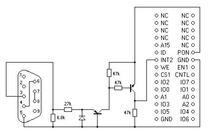
Circuit diagram of an interface for an RS232 port. It can only load data to the calculator.
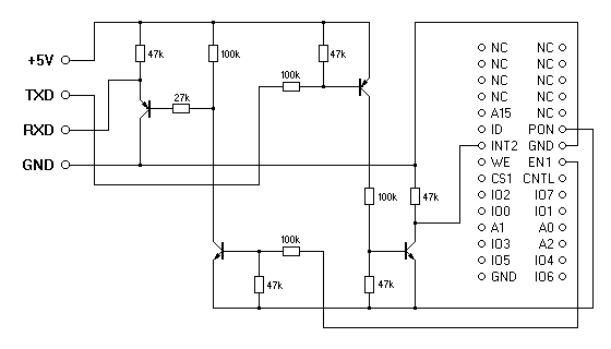
Circuit diagram of an interface with 5V voltage levels. In order to be used with an RS232 or USB port, an additional converter is required, for example built around the MAX232 level shifter (RS232) or the FT232R chip (USB).
The communication programs are written in assembler. The method of entering and executing machine code on the FX-8000G is described on a separate page.
The program reads data from the serial port to the file editor area. The transfer is terminated when the DEL key was pressed, or when transmission error occurred.
  2→S
  Hex
  60B78A40:Prog 0
  C00041C7:Prog 0
  7C600F99:Prog 0
  4802C300:Prog 0
  C0847114:Prog 0
  49F9822C:Prog 0
  82087C5A:Prog 0
  FA41081A:Prog 0
  0BF10174:Prog 0
  5B085EF1:Prog 0
  0FF9820C:Prog 0
  82082B82:Prog 0
  01FE00FA:Prog 0
  FA03F101:Prog 0
  745B088C:Prog 0
  000BF101:Prog 0
  745B25F9:Prog 0
  822C8208:Prog 0
  7C5AFA70:Prog 0
  B1880000:Prog 0
The timing critical parts are marked by the number of clock cycles in the comments. Please don't change them unless you know what you are doing!
        ORG     &H5AE8

BEGIN:  CAL     &HB78A          ;"LOAD executing"
        LDW     IX,&HC000
        LDW     IY,&HC77C
        CAL     &H0F99          ;fill RAM from address IX to IY with &HFF
        ADW     IX,2            ;IX = &HC77D
        PST     IE,&H00         ;disable interrupts
        PST     KO,&H84         ;select the keyboard output KO9
; wait for the start bit
LOOP1:  JMP     K,&H1449        ;10 cycles, "Break" when DEL key was pressed
; it should take ca. 1.5*379 clock cycles from this point up to BIT1
        GST     R2,IF           ;8 cycles
        TAN     R2,&H08         ;10 cycles
        JMP     Z,LOOP1         ;10 cycles
; start bit detected
        LDW     IY,&H081A       ;10 cycles, R121 = bit counter, R57 = delay
; bit loop, should take 379 clock cycles from this point up to STORE
LOOP2:
DEL2:   SB      R57,1           ;10 cycles
        JMP     NZ,DEL2         ;10 cycles
        LD      R57,15          ;10 cycles, delay
; it should take 379 clock cycles from this point up to STOP1
BIT1:   GST     R2,IF           ;8 cycles
        AN      R2,&H08         ;10 cycles
        TSB     R2,1            ;10 cycles, received bit -> Carry
        ROD     R0              ;8 cycles, R0 = received byte
        NOP                     ;6 cycles
        NOP                     ;6 cycles
; next bit
        SB      R121,1          ;10 cycles
        JMP     NZ,LOOP2        ;10 cycles
; store the received byte
STORE:  ST      -(IX),R0        ;16 cycles
DEL3:   SB      R57,1           ;10 cycles
        JMP     NZ,DEL3         ;10 cycles
; check for the stop bit
STOP1:  GST     R2,IF
        TAN     R2,&H08
        JMP     Z,LOOP1         ;next byte if no framing error
        JMP     &HB188          ;"I/O error"
The program dumps the RAM contents through the serial port. The transfer can be terminated with the DEL key.
  2→S
  Hex
  60B77B40:Prog 0
  C000C300:Prog 0
  C0847114:Prog 0
  495E8203:Prog 0
  A801FC81:Prog 0
  405F8B90:Prog 0
  0B830174:Prog 0
  5B00FE02:Prog 0
  FE01775B:Prog 0
  12C10070:Prog 0
  5AFDC101:Prog 0
  745AFD23:Prog 0
  F0E0775A:Prog 0
  F2701449:Prog 0
        ORG     &H5AE8

BEGIN:  CAL     &HB77B          ;"SAVE executing"
        LDW     IX,&HC000
        PST     IE,&H00         ;disable interrupts
        PST     KO,&H84         ;select the keyboard output KO9
; byte loop
LOOP1:  JMP     K,&H1449        ;"Break" when DEL key was pressed
        LD      R2,&H03         ;2 stop bits
        LD      R1,(IX)+
        BIUM    R1..R2          ;start bit
; bit loop, should take 379 clock cycles (=910000kHz/2400baud)
LOOP2:  LDM     R3..R4,16       ;14 cycles, dummy load to R4
DEL:    SB      R3,1            ;10 cycles
        JMP     NZ,DEL          ;10 cycles
; Carry cleared at this point
        ROD     R2              ;8 cycles
        ROD     R1              ;8 cycles, transmitted bit -> Carry
        JMP     C,ONE           ;10 cycles
        PST     IF,&H00         ;8 cycles
        JMP     LOOP2           ;10 cycles, next bit
ONE:    PST     IF,&H01
        JMP     NZ,LOOP2        ;next bit
; next byte
        TSB     R120,&HE0       ;end of the RAM?
        JMP     C,LOOP1         ;next byte if not
        JMP     &H1449          ;"Break"