| Index | wersja polska |
Signal naming according to the "PB-1000 technical handbook" published by the MODERN CO, LTD, Japan.
Credits to BLUE for his great help.

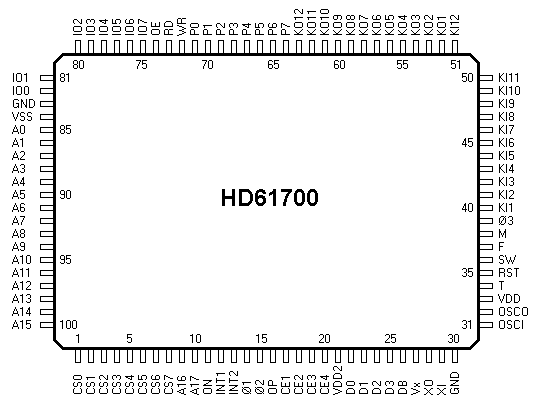
| Pin | Symbol | Function |
|---|---|---|
| 1..8 | CS0..CS7 | Chip select signals, active low.
Following address ranges are decoded: CS0: &H08000..&H0FFFF, ROM 32kB CS1: &H04000..&H05FFF, goes to the expansion port, unused CS2: &H06000..&H07FFF, internal RAM 8kB CS3: &H18000..&H19FFF, additional RAM module CS4: &H1A000..&H1BFFF, additional RAM module CS5: &H1C000..&H1DFFF, additional RAM module CS6: &H1E000..&H1FFFF, additional RAM module CS7: &H00C00..&H00C0F, serial, printer and FDD interface |
| 9,10 | A16,A17 | two most significant bits of the address bus |
| 11 | ON | ON interrupt request input, receives low level pulses of frequency 55 Hz from the pin 27 of the HD44352 LCD controller chip, the handle routine starts at the address &HFFCA |
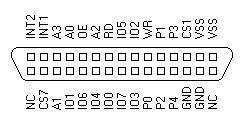
| 12 | INT1 | edge sensitive interrupt request input, connected to the peripheral port, the handle routine starts at the address &HFFBB |
| 13 | INT2 | level sensitive interrupt request input, connected to the peripheral port, the handle routine starts at the address &HFFD0 |
| 14..25 | Ø1,Ø2 OP CE1..CE4 VDD2 D0..D3 |
LCD controller bus, similar as in the Casio FX-700P, all signals use negative logic, pins CE3 and CE4 are not connected in the Casio PB-1000 |
| 26 | DB | jumper E to VSS (open), low level selects debug mode |
| 27 | Vx | filter capacitor 0.47uF for the 32768Hz oscillator supply voltage |
| 28,29 | XO,XI | crystal 32768Hz, XO is the output from the inverting oscillator amplifier |
| 30 | GND | connected to GND |
| 31,32 | OSCI,OSCO | ceramic resonator 910kHz, OSCO is the output from the inverting oscillator amplifier |
| 33 | VDD | internal logic power supply, outputs low level when the power is on, controls the Poff input of the voltage converter chip SCI7661 (through an inverter built with a pnp transistor) |
| 34 | T | connected either to GND through the jumper A (soldered) or to VSS through the jumper C (open), low level selects the test mode |
| 35 | RST | Reset input, active low, pressing the RESET button connects this pin to VSS |
| 36 | SW | Power on interrupt request input, connected by the Power switch either to VSS (power on) or to GND (power off), the handle routine starts at the address &HFFC1 |
| 37 | F | this output informs whether the clock is divided by 16 high level: slow mode, low level: fast mode (opposite to the description in the "technical handbook") |
| 38 | M | operation code fetch signal in the debug mode |
| 39 | Ø3 | bus reading signal in the debug mode |
| 40..51 | KI1..KI12 | keyboard matrix input port, can be accessed through the KY register KI5 can be optionally connected to VSS through the jumper B (open), purpose unknown |
| 52..63 | KO1..KO12 | keyboard matrix output port, controlled by the IA register |
| 64..71 | P7..P0 | The 8-bit bi-directional port which can be accessed through the PD and PE registers.
Function of individual bits: P7,P6 drive the piezo-buzzer P5 senses the supply voltage P4 is the reset output for peripherals P3 controls the FDD power, 0 turns the power on P2 selects the FDD transfer direction, 1 when writing to the FDD interface, 0 when reading from the FDD interface P1 is connected to the expansion port, but not used P0 is the FDD transfer direction acknowledge input |
| 72 | WR | bus write strobe signal, active low |
| 73 | RD | bus read strobe signal, active low |
| 74 | OE | output enable for external memory, looks like the Motorola scheme data strobe control signal E, not used in the PB-1000 (except perhaps by some external peripherals) |
| 75..82 | IO7..IO0 | bi-directional data bus |
| 83 | GND | positive supply voltage rail |
| 84 | VSS | negative supply voltage rail |
| 85..100 | A0..A15 | address bus |
The diagram illustrates the system bus and the LCD port waveforms taken while executing following program:
8E35: 54 00 C3    PPO &HC3
8E38: 52 0D       STL &H0D ;data &H0D is transferred in two cycles,
                           ;the least significant nibble first
8E3A: 27 00       PHU $0   ;data &H7A written to address &H6A2F


The columns of the keyboard matrix are driven from the 12-bit KO output port, controlled by the IA register. A pressed key makes contact between selected column and row. The rows are sensed by the 12-bit KI input port, accessible through the KY register.

Mapping of the KY register bits to the keyboard rows:
![]()


Images contributed by Mahmoud Yassine.